supply concepts logo header

What is a car wiring harness?

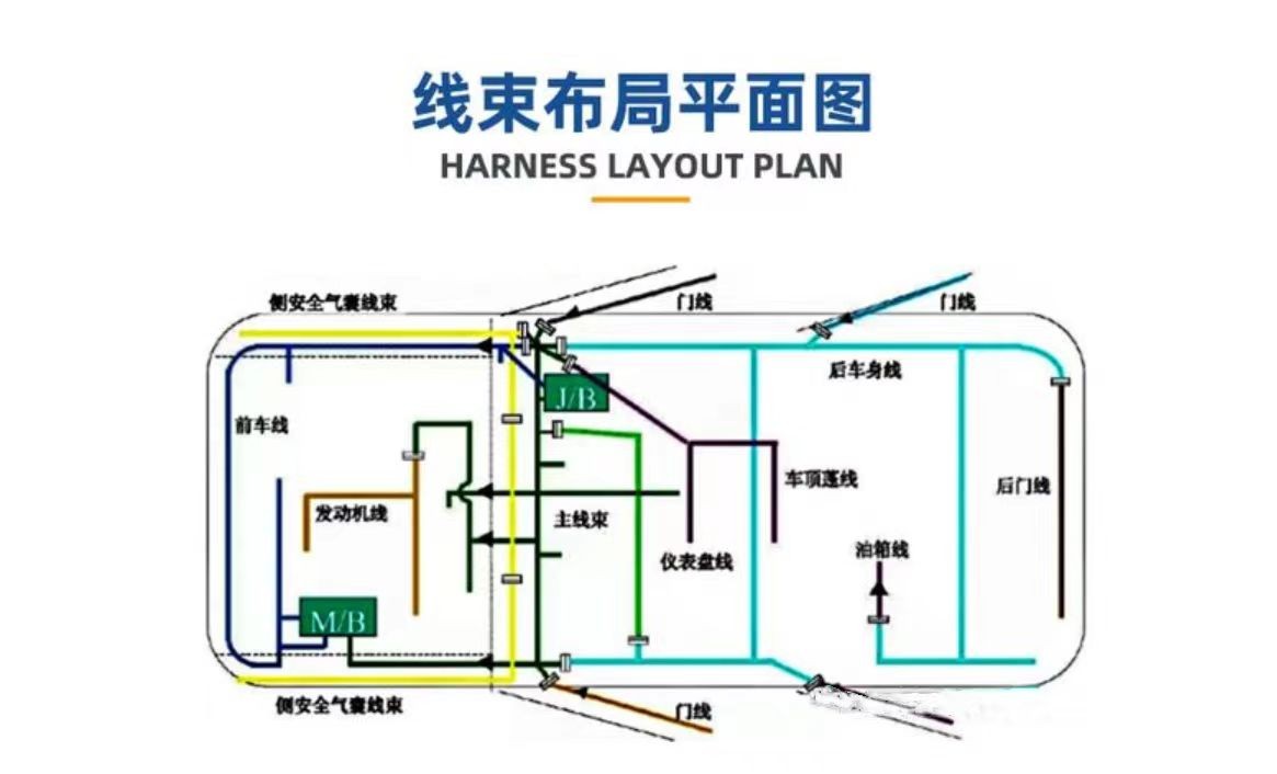
The automobile wiring harness is the network main body of the automobile circuit. Without the wiring harness, there would be no automobile circuit. At present, whether it is a high-end luxury car or an economical ordinary car, whether it is a simple wiring harness or a complex wiring harness, the form is generally similar, and they are all composed of wires, connectors, protective sleeves and positioning parts.

They play the role of connection and power supply, ensuring the normal operation of the vehicle and the normal operation of various electronic devices. Automobile wiring harness has various functions. First of all, it plays the role of connecting electrical equipment. In the engine compartment of the car, various sensors, motors and electronic control modules need to be connected through wiring harnesses to achieve information transmission and interaction.

Secondly, the wiring harness is also responsible for transmitting power signals and providing power support for various systems, such as ignition systems, lighting systems, air conditioning systems, etc. Most importantly, the wiring harness can also prevent damage to the wires caused by friction, vibration or moisture, improving the stability and safety of the vehicle.

Thread colors in automotive wiring harnesses

Thread colors in automotive wiring harnesses

Wire color: In order to facilitate the maintenance of automobile electrical systems, low-voltage wires are usually distinguished by different colors. The color of the wire insulation layer used today is generally two-color, consisting of a primary color and a secondary color. The main color is the base color of the wire, and the secondary color is the axial stripe color stripe on the wire. Commonly used colors are red, yellow, blue, green, black, white, brown, purple, gray, etc.
2D transition metal dichalcogenide (TMD) semiconductors

I’m excited about the potential of 2D transition metal dichalcogenides (TMDs) to shape transistor technology. The buzz around pursuing smaller, more efficient transistors has led to a deep interest in using 2D TMDs instead of Si Gate all-around (GAA) nanoribbons (NRs) below the 10nm gate length. At this tiny scale, Si faces issues like direct tunneling causing leakage, while 2D TMDs step in with their solid band gap and sustained mobilities, offering solutions to these hurdles. In the GAA NR structures, 2D TMDs showcase a scaling advantage: you can fit six 2D TMD NRs for every four Si NRs, potentially hinting at superior performance in the same space. These inherent physical benefits promise significant scaling potential.

Fabricating 2D TMD GAA NRs requires key steps like deposition, etching to form channels, doping, and contact/gate formation. However, each stage faces obstacles compared to established Si approaches. Etching TMD layers into nano-channels risks edge defects affecting performance and relies on selective chemistries that avoid harming delicate monolayers. Forming quality contacts requires optimizing exposed TMD surface area while minimizing material degradation from etching, unlike Si, conventional ion implantation doping methods damage TMDs, necessitating remote charge-based approaches that introduce coulombic scattering. Depositing effective gate oxides also struggle for a lack of dangling bonds to initiate controlled growth. Additionally, the overall mechanical fragility of atomically thin TMDs makes them vulnerable to internal stresses during processing.

Realizing the promise of 2D TMDs necessitates advancing their growth quality closer to the epitaxial precision of Si GAA NRs. Silicon’s unmatched defect densities have enabled its perseverance as the material of choice for over 50 years. Lateral growth from random nucleation sites results in polycrystalline morphologies with performance-sapping grain boundaries. Compounding this issue is the conflict between existing approaches to tackle contact resistance, primarily based on evaporated top contacts and the implicit preference for edge contacts in the simplest fabrication of NR transistors. A potential solution involves altering etch sequences to form a partial wrap-around contact, albeit potentially impacting transistor density.

Advancements in 2D TMD growth, contact resistance mitigation, and innovative fabrication techniques will likely pave the way for these materials to revolutionize the semiconductor industry, potentially rivaling or outperforming the capabilities of Si-based technology. 

Reference: O’Brien, K. P., Naylor, C. H., Dorow, C., et al. (Year). Process integration and future outlook of 2D transistors. DOI: https://doi.org/10.1038/s41467-023-41779-5